
CoCo 3 GIME Chip Reference
Edited from John Kowalski’s original web page “Sock Master’s GIME register reference”
People keep looking for GIME information, but it seems that there is no place you can find it on the web. So, I’ve decided to try to put together some GIME data so CoCo programmers could put it to good use.
The GIME is a custom chip designed to replace a number of parts from the CoCo 1&2 and also add extra CoCo 3 specific features. For now, at least, I’ll concentrate mostly on CoCo 3 features. The CoCo 1&2 features work the same as before, so you can probably find that information on other web sites.
Interrupt Vectors
Here’s a table of the interrupt vectors and where they end up going. You can’t change the $FFxx vectors, but you can change the $FExx and $01xx vectors which contain jmps/lbras to the interrupt routine.
| Interrupt | CPU reads | which points to | which jumps to this routine |
|---|---|---|---|
| SWI3 | $FFF2 | $FEEE | $0100 |
| SWI2 | $FFF4 | $FEF1 | $0103 |
| FIRQ | $FFF6 | $FEF4 | $010F |
| IRQ | $FFF8 | $FEF7 | $010C |
| SWI | $FFFA | $FEFA | $0106 |
| NMI | $FFFC | $FEFD | $0109 |
| RESET | $FFFE | $8C1B |
$FF90 (65424) Initialization Register 0 – INIT0
| Bit 7 | COCO | 1=CoCo 1/2 compatible mode |
| Bit 6 | MMUEN | 1=MMU enabled |
| Bit 5 | IEN | 1=GIME chip IRQ enabled |
| Bit 4 | FEN | 1=GIME chip FIRQ enabled |
| Bit 3 | MC3 | 1=RAM at FExx is constant (secondary vectors) |
| Bit 2 | MC2 | 1=standard SCS (spare chip select) |
| Bits 1-0 | MC1 MC0 |
ROM map control 0x=16K internal, 16K external 10=32K internal 11=32K external (except interrupt vectors) |
To use CoCo 3 graphics (even modes that visually resemble CoCo 1/2 modes), the COCO bit must be set to zero. When using CoCo 1/2 native modes, the bit is set to 1. RSDOS typically sets the INIT0 register to 196 in CoCo 2 resolutions and 68 when using CoCo 3 graphics modes.
$FF91 (65425) Initialization Register 1 – INIT1
| Bit 7 | Unused | |
| Bit 6 | ? | Memory type 1=256K, 0=64K chips |
| Bit 5 | TINS | Timer clock source 1=279.365 nsec, 0=63.695 usec |
| Bits 4-1 | Unused | |
| Bit 0 | TR | MMU task select 1=enable $FFA8-$FFAF MMU registers 0=enable $FFA0-$FFA7 MMU registers |
The TINS bit selects the clock speed of the countdown timer. The 279 ns clock is useful for interrupt driven sound routines while the 63 us clock is used for a slower timer. The task bit is generally set to zero in DECB. The task register select which set of MMU bank registers to assign to the CPU’s 64K workspace.
$FF92 (65426) Interrupt request enable register – IRQENR
$FF93 (65427) Fast interrupt request enable register – FIRQENR
| Bits 7-6 | Unused | |
| Bit 5 | TMR | 1=Enable timer interrupt |
| Bit 4 | HBORD | 1=Enable Horizontal border interrupt |
| Bit 3 | VBORD | 1=Enable Vertical border interrupt |
| Bit 2 | EI2 | 1=Enable Serial data interrupt |
| Bit 1 | EI1 | 1=Enable Keyboard interrupt |
| Bit 0 | EI0 | 1=Enable Cartridge interrupt |
TMR: An interrupt is generated whenever the 12 bit timer counts down to zero.
HBORD: A horizontal border interrupt is generated on the falling edge of HSYNC.
VBORD: A vertical border interrupt is generated on the falling edge of VSYNC.
EI2: A serial interrupt is generated on the falling edge of the signal on PIN 4 of the serial port.
EI1: A keyboard interrupt is generated whenever a zero appears on any one of PA0-PA6 on the PIA0.
EI0: A cartridge interrupt is generated on the falling edge of the signal on PIN 8 of the cartridge port.
Reading from the register tells you which interrupts came in and acknowledges and resets the interrupt source.
$FF94 (65428) Timer register MSB
| Bits 7-4 | Unused | |
| Bits 3-0 | TMRH | Timer bits 8-11 |
$FF95 (65429) Timer register LSB
| Bits 7-0 | TMRL | Timer bits 0-7 |
Historic assertions in their plain English form are currently being re-investigated to see if there is more to the story due to recent discoveries.
- The 12 bit Timer Register can be loaded with any number from 0-4095.
- The timer resets and starts counting down as soon as a number is written to $FF94 (writing to $FF95 does not restart the timer, but the value saves as the LSB).
- The Timer Register is write-only, meaning that nothing useful can be expected when reading the register, nor does reading from either Timer Register byte restart the timer.
- When the Timer Counter reaches zero, it triggers an interrupt (if enabled) then automatically restarts to the value of the Timer Register.
- Setting the Timer Register to $000 stops the timer from operating, sort of. An interrupt will be generated almost immediately when setting the IRQ or FIRQ Enable bits.
- The Timer Register also controls the rate of blinking text. When the Timer Register is set to $000, any blinking text will freeze in its current state (visible or invisible). Whether or not the programmer can control what state the blinking text appears should be an exercise for you.
- The text “blink-toggle” happens at (timer rate / 4). That is, for every 4 timer interrupts (or countdowns to zero), the blink on/off state alternates.
- The timer works slightly differently on both 1986 and 1987 versions of the GIME. Neither can actually run a clock count of 1. That is, if you store a 1 into the Timer Register, the 1986 GIME actually processes this as a ‘3’ and the 1987 GIME processes it as a ‘2’. All other values stored are affected the same way : nnn+2 for 1986 GIME and nnn+1 for 1987 GIME. This is currently being investigated by as possibly being a one-clock delay in the 1986 GIME combined with 1 clock of signal propagation in both GIMEs, since actually adding 1 or 2 should overflow the 12-bit timer yet no overflow situations have been observed.
- The reasoning behind the GIME “updating” the whole 12-bit timer rate whenever the MSB is written to instead of the LSB is unknown. The 6809 CPU writes the MSB before the LSB when storing a 16-bit value, which means the programmer probably needs to write the LSB then the MSB, but not both using a 16-bit Store instruction. For example, if you want to set the timer to 0 ($000) to stop it, would a STX, STY, STD immediately stop the timer, or only after the current counter reaches 0? Try it and see.
- It’s apparent that the GIME designer(s) were thinking in “little endian” when it came to setting the timer rate.
- Why did the designers choose a 12-bit timer instead of any other range?
$FF96 (65430) Reserved
| Bits 7-0 | Unused |
$FF97 (65431) Reserved
| Bits 7-0 | Unused |
$FF98 (65432) Video mode register – VMODE
| Bit 7 | BP | 1=Graphics modes 0=Text modes |
| Bit 6 | Unused | |
| Bit 5 | BPI | 1=Composite color phase invert |
| Bit 4 | MOCH | 1=Monochrome on Composite video out |
| Bit 3 | H50 | 1=50Hz video 0=60Hz video |
| Bits 2-0 | LPR | 00x=one line per row 010=two lines per row 011=eight lines per row 100=nine lines per row 101=ten lines per row 110=eleven lines per row 111=*infinite lines per row |
*Mostly useless, but it does generate a graphics mode where the whole screen is filled with the same line of graphics – like a 320×1 resolution. This can be used for a very fast oscilloscope type display where the program only updates data in one scan line over time and as the screen refreshes, you get a screen full of samples. I also used it in my Boink bouncing ball demo to take manual control of the vertical resolution of the screen to make the ball appear that it’s going up and down (without actually scrolling the whole screen up and down).
$FF99 (65433) Video resolution register – VRES
| Bit 7 | Unused? | |
| Bits 6-5 | LPF | 00=192 scan lines on screen 01=200 scan lines on screen 10=*zero/infinite lines on screen (undefined) 11=225 scan lines on screen |
| Bits 4-2 | HRES | Horizontal resolution using graphics: 000=16 bytes per row 001=20 bytes per row 010=32 bytes per row 011=40 bytes per row 100=64 bytes per row 101=80 bytes per row 110=128 bytes per row 111=160 bytes per row When using text: 0x0=32 characters per row 0x1=40 characters per row 1×0=64 characters per row 1×1=80 characters per row |
| Bits 1-0 | CRES | Color Resolution using graphics: 00=2 colors (8 pixels per byte) 01=4 colors (4 pixels per byte) 10=16 colors (2 pixels per byte) 11=Undefined (would have been 64 or 256 colors?) When using text: x0=No color attributes x1=Color attributes enabled |
*The zero/infinite scanlines setting will either set the screen to display nothing but border (zero lines) or graphics going all the way up and down out of the screen, never retriggering. It all depends on when you set the register. If you set it while the video raster was drawing the vertical border you get zero lines, and if you set it while video was drawing graphics you get infinite lines. Mostly useless, but it should be possible to coax a vertical overscan mode using this with some tricky timing.
| HRES | CRES | Commonly used graphics modes |
|---|---|---|
| 111 | 01 | 640 pixels, 4 colors |
| 101 | 00 | 640 pixels, 2 colors |
| 110 | 01 | 512 pixels, 4 colors |
| 100 | 00 | 512 pixels, 2 colors |
| 111 | 10 | 320 pixels, 16 colors |
| 101 | 01 | 320 pixels, 4 colors |
| 011 | 00 | 320 pixels, 2 colors |
| 110 | 10 | 256 pixels, 16 colors |
| 100 | 01 | 256 pixels, 4 colors |
| 010 | 00 | 256 pixels, 2 colors |
| 101 | 10 | 160 pixels, 16 colors |
| 011 | 01 | 160 pixels, 4 colors |
| 001 | 00 | 160 pixels, 2 colors |
| 100 | 10 | 128 pixels, 16 colors |
| 010 | 01 | 128 pixels, 4 colors |
| 000 | 00 | 128 pixels, 2 colors |
$FF9A (65434) Border color register – BRDR
| Bits 7-6 | Unused | |
| Bits 5-0 | BRDR | Border color |
This controls the color of the border around the screen. The color bits work the same as the palette registers. This register only controls the border color of CoCo 3 video modes and does not affect Coco 1/2 modes.
$FF9B (65435) Reserved
| Bits 7-2 | Unused | |
| Bits 1-0 | VBANK | Used by Disto 2 Meg upgrades to switch video between 512K banks |
$FF9C (65436) Vertical scroll register – VSC
| Bits 7-4 | Unused | |
| Bits 3-0 | VSC | Vertical smooth scroll. |
The vertical scroll register is used to allow smooth scrolling in text modes. Consecutive numbers scroll the screen upwards one scan line at a time in video modes where more than one scan line makes up a row of text (typically 8 lines per character row) or graphics (double height+ graphics).
$FF9D (65437) Vertical offset register MSB
| Bits 7-0 | Y15-Y8 | MSB Start of video in RAM (video location * 2048) |
$FF9E (65438) Vertical offset register LSB
| Bits 7-0 | Y7-Y0 | LSB Start of video in RAM (video location * 8) |
Y15-Y0 is used to set the video mode to start in any memory location in 512K by steps of 8 bytes. On a 128K machine, the memory range is $60000-$7FFFF. There is a bug in some versions of the GIME that causes the computer to crash when you set odd numbered values in FF9E in some resolutions, so it’s safest to limit positioning to steps of 16 bytes. Fortunately, you can use FF9F to make up for it and get steps as small as 2 bytes.
$FF9F (65439) Horizontal offset register
| Bit 7 | HVEN | 1=Horizontal virtual screen enable (256 bytes per row) 0=Normal horizontal display |
| Bits 6-0 | X6-X0 | Horizontal offset address (video location *2) |
You can combine the horintal and vertical offsets to get a higher definition video position:
Y15-Y4,X6-X0 which gives you 19 bit positioning by steps of 2 bytes.
Otherwise, you can use this register to do scrolling effects. The virtual screen mode allows you to set up a 256 byte wide graphics or text screen, showing only part of it at a time and allowing you to scroll it vertically.
$FFA0-$FFA7 (65440-65447) MMU bank registers (Task 0)
$FFA8-$FFAF (65448-65455) MMU bank registers (Task 1)
| $FFA0/$FFA8 | Bank at $0000-$1FFF |
| $FFA1/$FFA9 | Bank at $2000-$3FFF |
| $FFA2/$FFAA | Bank at $4000-$5FFF |
| $FFA3/$FFAB | Bank at $6000-$7FFF |
| $FFA4/$FFAC | Bank at $8000-$9FFF |
| $FFA5/$FFAD | Bank at $A000-$BFFF |
| $FFA6/$FFAE | Bank at $C000-$DFFF |
| $FFA7/$FFAF | Bank at $E000-$FFFF (or $E000-$FDFF if Constant Page RAM enabled) |
- Task 0 MMU registers are enabled when the task bit (FF91) is clear.
- Task 1 MMU registers are enabled when the task bit (FF91) is clear.
- The MMU registers allocate blocks of 8K into the CPU’s 64K workspace.
- Valid bank ranges are 56-63 on 128K machines, 0-63 on 512K machines, 0-127 on 1Meg machines and 0-255 on 2Meg machines.
- The registers can be read, but the upper 2 bits must be masked out as they return bleedover from the bus (sometimes zero, sometimes one). This is okay for machines with 512K or less, but poses a problem for 1Meg and up. Supposedly some memory upgrades fixed this, but most don’t so you can’t rely on those 2 bits to be there when you read the registers.
In ROM/RAM mode, MMU blocks $3C-$3F don’t access RAM. They access either internal or external ROM. The RAM/ROM mode is entered by writing any value to address $FFDE. RAM mode is selected by writing any value to address $FFDF.
In ROM/RAM mode there are three different ROM configurations available. They are selected by setting bits 1 and 0 of address $FF90 to:
| $3C | $3D | $3E | $3F | Bit Value |
|---|---|---|---|---|
| Extended Color BASIC | Color BASIC | 16K Cartridge ROM | 0X | |
| Extended Color BASIC | Color BASIC | Reset Initialization | Super Extended Color BASIC | 10 |
| 32K Cartridge ROM | 11 | |||
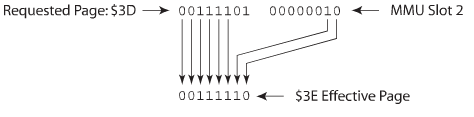 The ROM pages ($3C-$3F) can be written to any of the eight available MMU slots. In all cases the last two bits of the page are ignored by the MMU and substituted by the last two bits of the slot number. For example, writing $3D to slot 2 of the MMU does not map the second 8k page of ROM to addresses $4000-$5FFF (it maps block $3E, the third ROM page). This essentially means that page $3C will only appear in slots 0 and 4; $3D in 1 and 5; $3E in 2 and 6; $3F in 3 and 7.
FFB0-FFBF (65456-65471) Color palette registers
| FFB0 | Color 0 | Bits 7-6 Unused Bit 5 = High order Red Bit 4 = High order Green Bit 3 = High order Blue Bit 2 = Low order Red Bit 1 = Low order Green Bit 0 = Low order Blue |
| FFB1 | Color 1 | same as above |
| FFB2 | Color 2 | … |
| FFB3 | Color 3 | |
| FFB4 | Color 4 | |
| FFB5 | Color 5 | |
| FFB6 | Color 6 | |
| FFB7 | Color 7 | |
| FFB8 | Color 8 | |
| FFB9 | Color 9 | |
| FFBA | Color 10 | |
| FFBB | Color 11 | |
| FFBC | Color 12 | |
| FFBD | Color 13 | |
| FFBE | Color 14 | |
| FFBF | Color 15 |
The color set when using composite monitors is different than above (which applies to RGB monitors). On composite displays, Bits 5-4 control 4 levels of intensity, and bits 3-0 control 16 hues of color.
These registers can also be read to determine what palettes are set but like the MMU registers, the upper 2 bits must be masked out. Both reading and writing to the palette registers causes a small ‘glitch’ on the screen. If you want to avoid them, you can change the palettes while the video is in the vertical or horizontal border.
On the other hand, you could also generate the glitches on purpose, to superimpose snow on the screen. The glitches appear as the color you set the register to (with a bit of the previous color setting at the beginning) and with precise CPU timing loops you could actually superimpose definable graphics over the screen this way.
FFD8/FFD9 (65496/65497) CPU clock rate
| FFD8 | ‘Slow poke’ | Any write selects 0.89 Mhz CPU clock |
| FFD9 | ‘Fast poke’ | Any write selects 1.79 Mhz CPU clock |
FFDE/FFDF (65502/65503) ROM/RAM map type
| FFDE | ROM mode | Any write switches system ROMs into memory map |
| FFDF | RAM mode | Any write selects all-RAM mode |
Click here to go to Sock Master’s Web Page.
